At Fidus Systems, we specialize in FPGA design and embedded system development, working closely with Lattice Semiconductor to leverage their MachXO5-NX FPGAs and cutting-edge design tools. In this blog, we’ll share our hands-on experience integrating LTPI and MIPI in Lattice FPGAs, overcoming design challenges, and demonstrating real-world applications.
If you’re designing for high-speed data transfer, system control, or embedded vision, this deep dive into LTPI and MIPI will provide key insights.
For a complete technical discussion and demonstration, watch our webinar.
LVDS Tunneling Protocol and Interface in FPGA-Based Systems
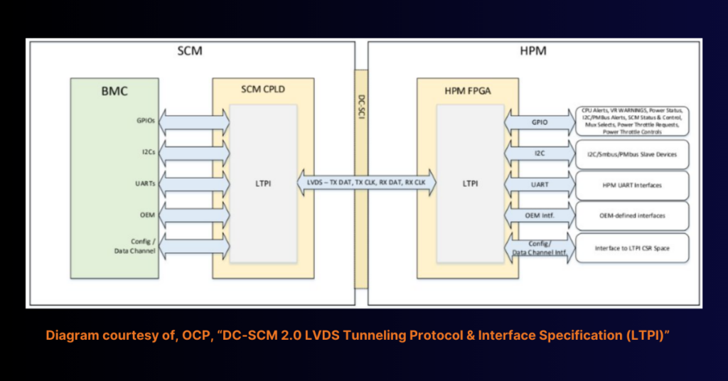
LTPI was developed as part of the Open Compute Project to enable high-speed, low-pin-count communication within data center architectures. It provides a scalable, low-latency transport mechanism for common control signals while minimizing PCB complexity. While LTPI was originally intended for interconnectivity between Secure Control Modules and Host Processor Modules in data centers, its capabilities make it highly suitable for FPGA-based systems requiring efficient control signal management and real-time data transfer.
LTPI operates using a frame-based approach to multiplex multiple low-speed control protocols onto a single LVDS link, reducing the number of required interconnects. It supports the tunneling of I2C for sensor/peripheral communication, UART for serial data transmission, and GPIO for both standard and low-latency signal control.
The LTPI frame is divided into various time slots, including the data channel for memory-mapped transactions, the OEM channel for user-defined data transport, and GPIO fields that allow both normal latency and low-latency signal transmission. This structure makes LTPI highly adaptable for applications beyond traditional data centers, particularly in embedded systems that require efficient control plane expansion.
LTPI is well-suited for FPGA and CPLD implementations, as its soft IP is available from multiple FPGA vendors. In the Lattice MachXO5-NX FPGA, LTPI achieves data rates of up to 1200 Mbps, utilizing a dual unidirectional LVDS interface consisting of a TX clock and TX data pair and an RX clock and RX data pair.
Mobile Industry Processor Interface for High-Speed Video Transmission
MIPI is widely used in mobile and embedded vision applications due to its low power consumption, high bandwidth, and minimal PCB footprint. In FPGA-based designs, MIPI enables efficient high-speed data transmission between image sensors, processors, and displays.
MIPI Camera Serial Interface 2 (CSI-2) is optimized for video streaming from image sensors to an FPGA. It supports data rates of several gigabits per second and utilizes I²C for configuration and high-speed lanes for data transport. MIPI Display Serial Interface 2 (DSI-2) facilitates video data transfer from an FPGA to a display, supporting high-resolution, full-color video output.
The different MIPI physical layers include D-PHY, C-PHY, and A-PHY. D-PHY is the most commonly used in FPGA applications, supporting high-speed SLVS signaling. C-PHY is emerging as an alternative for higher data rates and increased efficiency. A-PHY is optimized for longer transmission distances, such as in automotive applications.
Implementation of LTPI and MIPI in an FPGA-Based Video Transport System
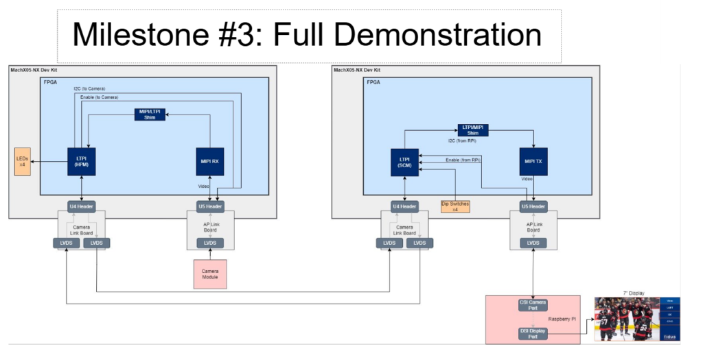
At Lattice DevCon 2024, Fidus Systems presented a real-world demonstration of LTPI-based high-speed video transmission using two Lattice MachXO5-NX FPGAs. The hardware setup consisted of two Lattice MachXO5-NX development kits, a Raspberry Pi 3B+ with a seven-inch display, a Raspberry Pi Camera Module, and Lattice Camera Link and AP Link breakout boards.
The system architecture involved an image sensor sending video data through a MIPI CSI-2 interface to the first FPGA, which functioned as the host processor module. The FPGA packaged the video data into LTPI frames and transmitted them over an LVDS connection to the second FPGA, acting as the secure control module. The second FPGA extracted the video data from the LTPI frames and sent it through a MIPI DSI-2 interface to a Raspberry Pi display. The Raspberry Pi software remained unaware that the camera was remotely connected, treating it as if it were directly attached.
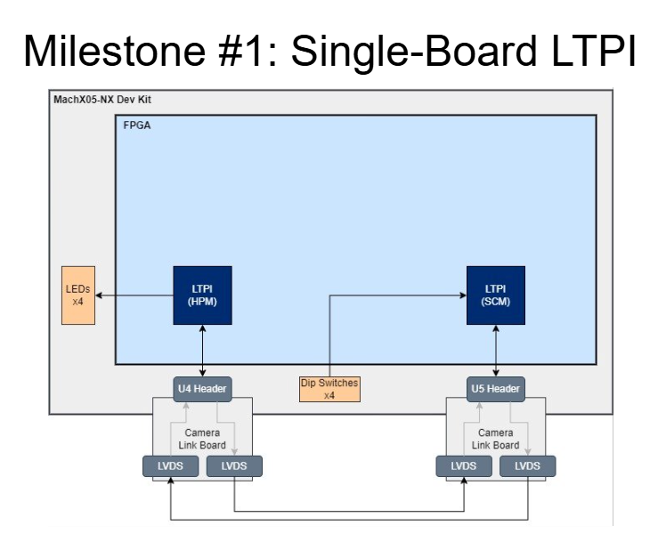
A milestone-based design strategy was used to develop this system, where individual components were validated separately before being integrated.
The first milestone involved implementing LTPI-based GPIO tunneling to control LEDs remotely
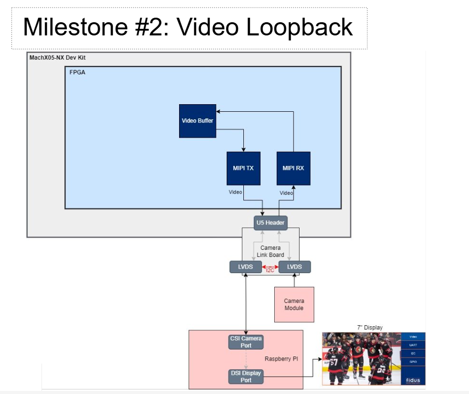
The second milestone focused on establishing a MIPI RX-to-TX loopback, confirming compatibility between the FPGA and Raspberry Pi.
Once these individual designs were validated, they were merged into the final demonstration.
Technical Challenges and Solutions
One of the primary challenges was determining the available bandwidth for LTPI-based video transmission. Using the 600 MHz maximum link speed of the Lattice LTPI IP core along with DDR allowed for an effective link speed of 1.2 Gbps. The frame rate of the LTPI link was calculated to be 7.5 MHz, with a new frame transmitted every 133 nanoseconds. The available bandwidth for video transmission was approximately 480 Mbps, which limited the achievable resolution and frame rate.
To maximize performance, Raw 10 encoding was used, as it required only 10 bits per pixel compared to 24 bits for eight-bit RGB. This allowed for a 640×480 resolution at 60 frames per second without exceeding bandwidth limitations.
Another challenge was adapting the LTPI OEM channel for video transport. The OEM pins are bi-directional and typically require direct FPGA pin access, making it difficult to drive them internally. To address this, the FPGA’s Versa connectors were used to loop back signals, allowing video data to be transmitted effectively.
Clock synchronization between LTPI and MIPI was also a critical consideration. Since the LTPI and MIPI interfaces operated at different clock rates, direct synchronization was not possible. A PLL-based clock domain crossing (CDC) approach was implemented, where the LTPI clock from the secure control module was used to drive the PLL in the host processor module. This ensured stable, lossless data transmission across the LTPI link.
Development Tools and Debugging Methodology
To develop and debug the system, several tools were used. Lattice Radiant was the primary tool for FPGA synthesis, IP core configuration, and bitstream generation. Questa Simulation Wizard was used to verify LTPI frame structures in a controlled pre-silicon environment. The Lattice Reveal Logic Analyzer was instrumental in real-time debugging, allowing signal monitoring and analysis within the FPGA.
A structured approach was followed, incorporating simulation, logic analysis, and hardware verification to ensure the successful integration of LTPI and MIPI. Test benches were iteratively refined to validate system behavior under different operating conditions.
Applications of LTPI and MIPI Beyond Data Centers
While LTPI was originally designed for data center applications, its capabilities make it highly relevant for embedded systems, industrial automation, and aerospace applications. LTPI reduces the number of interconnects required for multi-FPGA communication, making it an attractive alternative to traditional serial buses. Its ability to multiplex low-speed control signals over a single high-speed link allows for greater system efficiency in automation and control applications.
MIPI’s role in high-speed, low-power data transport makes it well-suited for embedded vision and AI-driven systems. The combination of LTPI and MIPI enable real-time video processing, making it an excellent choice for automotive vision systems, robotics, and AI-enhanced industrial inspection.
As FPGA architectures continue to evolve, LTPI and MIPI are expected to gain wider adoption in applications that require efficient control and high-bandwidth data transmission.
Conclusion
The integration of LTPI and MIPI in FPGA-based embedded systems provides a scalable, efficient solution for high-speed control and data transport. The successful demonstration at Lattice DevCon 2024 highlights LTPI’s versatility beyond data centers and its applicability in industrial automation, embedded AI, and multi-FPGA architectures.
1. Can LTPI be adapted for applications outside of data centers, such as automation or aerospace?
Yes, LTPI is highly adaptable beyond data centers. While originally designed for secure module-to-processor communication in data centers, its ability to multiplex low-speed control signals over a high-speed LVDS link makes it valuable in industrial automation, aerospace, and embedded systems. It can reduce backplane interconnect complexity, extend control signals across multiple FPGAs, and create efficient software-controlled interfaces in multi-FPGA environments.
2. How did you ensure synchronization between the LTPI and MIPI clock domains?
Synchronization between LTPI and MIPI was achieved using a clock domain crossing FIFO to transfer data while preventing timing mismatches. Additionally, due to PLL limitations in the FPGA, a shared reference clock was used to ensure stable timing for both LTPI and MIPI signals. This approach prevented data loss and ensured consistent video streaming over the LTPI link.
3. What development tools were used during the LTPI demonstration?
The primary tools used were:
Lattice Radiant for FPGA synthesis, IP core configuration, and bitstream generation.
Questa Simulation Wizard for verifying LTPI frame structures and debugging timing issues.
Lattice Reveal Logic Analyzer for real-time debugging and capturing data flows within the FPGA. These tools were critical in debugging, ensuring seamless integration, and validating the performance of LTPI and MIPI in the demonstration.
How Embedded Systems Outsourcing Differs from Software Outsourcing?
Software outsourcing has a mature playbook. It starts breaking the moment hardware enters the picture. Here is where embedded engagements diverge on toolchains, testing, and the cost of an error, and how to adjust your vendor management before a firmware bug turns into a board respin.
How Do You Deploy a Person Re-Identification Application on AMD Ryzen™ AI?
Discover how Fidus’ Person Re-Identification demo on a Ryzen™ AI–based SAPPHIRE EDGE AI Mini-PC highlights AI integration, optimization, custom-data training, and repeatable testing for faster product development.