
FPGA and RF engineering services or a new hire: How to decide
Engineering is the hardest role in aerospace and defense to fill. Three questions show whether your FPGA or RF gap needs a new hire or FPGA engineering services.
Back to top

What a dense AMD Zynq™ UltraScale+™ RFSoC system-on-module taught us about power, thermal, and signal integrity in industrial environments.
An industrial vision and motion-control customer came to us with a short brief: take the converter performance of the AMD Zynq UltraScale+ RFSoC and make it small enough to drop into somebody else’s system.
They wanted a system-on-module. On it: the RFSoC itself, LPDDR4, MRAM, flash, an SD card interface, an Ethernet PHY, and a spread of general peripheral I/O, including RGMII, SPI, and differential pairs. It had to survive an industrial enclosure with no airflow. And it had to land at 65 x 65 mm.
We finished at 65 x 90 mm. That extra 25 mm is the most interesting number in the project, because of where it went and what it bought. The point of the exercise is worth stating plainly. An RFSoC puts RF-class ADCs and DACs on the same device as the processing system and programmable logic. Getting that combination into a sealed, fanless industrial product, rather than a rack or a fan-cooled chassis, is what the rest of this is about.
| Device | AMD Zynq UltraScale+ RFSoC |
| Footprint | 65 x 90 mm (target was 65 x 65 mm) |
| Stack-up | 20 layers, 94 mils overall thickness |
| Memory | LPDDR4 at 4.2 Gbps |
| Also on module | MRAM, flash, SD 3.0, Ethernet PHY, RGMII, SPI, differential pairs |
| Cooling | None on module. Sealed industrial enclosure, no airflow |
| Fidus scope | Schematic, layout, signal integrity, hardware test |
| Delivery | ~10 months, team of 17, fixed price, on time and on budget |
Before a single schematic page was drawn, we laid the module out in Visio. A rough two-dimensional puzzle of every component we knew we needed, against the area we had been given. It took a day and it told us two things.
First, that 65 x 65 mm was going to be extremely tight. Second, and more usefully, it told us why. The power solution, not the RFSoC or the memory, was the thing consuming the area.
| Target | As built | |
|---|---|---|
| Footprint | 65 x 65 mm | 65 x 90 mm |
| Board area | 4,225 mm² | 5,850 mm² (+38%) |
| What set the limit | The power solution, not the RFSoC or the memory | |
| What the extra area bought | Signals the customer had originally cut, added back | |
That let us have the size conversation with the customer at the start of the project rather than three months in, when a form-factor change is expensive. They accepted 65 x 90 mm early, and used the extra room to add signals they had originally cut. It also meant layout could start almost immediately, because the placement strategy was already settled.
If you are integrating an RFSoC into a constrained form factor, budget the placement study before design kickoff. It is cheap, and it moves the hardest conversation to the point where it costs the least.
The Zynq UltraScale+ RFSoC integrates RF-class ADCs and DACs directly alongside the processing system and programmable logic. That integration is the reason to choose the part. It is also the reason the power design dominates the board.
Converter supply rails do not behave like digital rails. Noise that would be invisible on a logic supply lands directly in the converter’s own noise floor, and the specifications we were designing to were far tighter than anything the digital side of the module needed, while still delivering several amps.
Two constraints pulled against each other. The rails needed to be quiet, which argues for linear regulation. The module needed to be small and thermally survivable with no airflow, which argues for switching regulation.
We went with a relatively new generation of TI switching regulators, backed by the vendor’s own application work, then added LDO post-regulation on the most sensitive rails.
input rail
          |
          v
  +-----------------+
  |    switching    |---->  digital rails
  |    regulator    |       (no post-reg needed)
  +--------+--------+
           |
           v
  +-----------------+
  |       LDO       |   <-- added for margin,
  | post-regulation |       not to meet spec
  +--------+--------+
           |
           v
   converter supply rails
   (RF-ADC / RF-DAC)
On paper the switchers alone met the noise budget. We did the extra analysis anyway and kept the post-filtering, partly for margin and partly because neither we nor the customer had lab equipment capable of proving the noise performance in isolation. The only real test was the customer running their own converters and measuring the result.
That is an uncomfortable position to design into, so we designed for adjustability. The rails include provisions to trim precision further if the system-level measurements demand it.
In a module this dense, every capacitor you add is area you take from something else.
The trade we accepted: minimum decoupling, tight component spacing, and more simulation time than a comparable design would normally justify. In a module this dense, every capacitor you add is area you take from something else.
The module runs LPDDR4 at 4.2 Gbps on a 20-layer stack-up, 94 mils thick. On a board this dense, routing memory and then discovering a margin problem is not recoverable in a schedule. There is nowhere to move the traces to.
So the signal integrity work ran pre-layout rather than as a post-layout check. The engineer running the LPDDR4 simulations also routed the interface, which is not always how these roles split. It meant the simulation results shaped the routing as it happened rather than judging it afterwards.

The module dissipates into a sealed industrial enclosure. There is no fan, and the heat sinking is done by the customer’s enclosure, not by anything we could mount. That constraint reaches back into the power architecture. Efficiency stops being an electrical preference and becomes a mechanical requirement, because every watt you waste is a watt somebody else’s chassis has to move.
One genuinely avoidable lesson. The design needed SD 3.0 mass storage. The RFSoC offers multiple pin options for the SD interface, but not all of them support boot, and we had not pinned down how the card would be used at boot until late. That combination forced a last-minute pinout change plus some surrounding logic on a board with no spare room.
The lesson is not “read the datasheet”. It is that on a highly integrated device, peripheral pin assignment is a system decision rather than a hardware one. Ask how every interface will be used, including at boot, before you commit placement.
Density has a cost that does not show up until bring-up. A large number of signals on this module route underneath the package, and with everything spaced tightly, there is very little to physically touch with a probe. We brought the module up on a separate breakout board, which is its own kind of constraint: you are debugging two unfamiliar things at once.
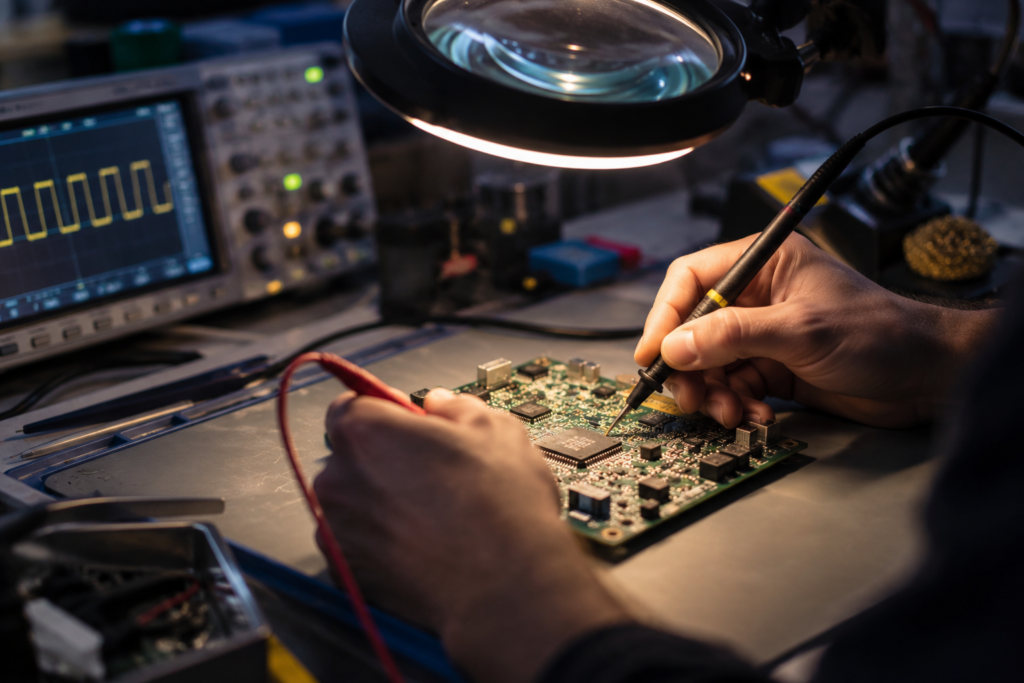
Where we would push harder next time is parametric testing of the power supplies. We would have liked to characterize the rails directly rather than infer their performance from system behavior.
The customer had the system architecture and knew their application. What they did not have in-house was the hardware and layout capacity to execute a board this dense, on this schedule.
Fidus took the whole hardware scope: schematic, layout, signal and power integrity, and hardware test, with the project management team. On a design like this that matters more than it sounds, because the power architecture, the placement strategy, and the signal integrity work are not separable problems.
The placement study reset the form factor in week one because the people who would route the board were the ones running it. The LPDDR4 interface was simulated before layout because the same engineer did both. Split those across vendors and the form-factor conversation happens in month three instead, when it costs real money.
Three things are reusable:
None of the individual problems here were exotic. What made the module hard was that they all had to be solved in the same 5,850 square millimetres, with no airflow and no room to iterate.

Fidus is a custom embedded systems design and services company and an AMD Premier Partner, delivering FPGA, hardware, signal and power integrity, embedded software, ASIC RTL design and verification, mechanical and thermal development, plus strategic manufacturing from prototype to low/mid volume.
Working on something this dense?
If you have an RFSoC that has to fit somewhere it doesn’t, a power budget that won’t close, or a memory interface you’d rather simulate than rework, tell us what you’re up against. You’ll get a straight answer on whether it’s doable and what it would take.

Engineering is the hardest role in aerospace and defense to fill. Three questions show whether your FPGA or RF gap needs a new hire or FPGA engineering services.

Earth observation launches are nearly tripling, but downlink capacity per spacecraft hasn't kept up. Deciding what to process in orbit is now a hardware decision made years before launch.

When should you outsource heterogeneous computing design? Keep the CPU, FPGA, GPU and NPU architecture call in-house, and get outside validation before board layout, while changing the partition is still cheap.
Trust us to deliver on time. That’s why 95% of our customers come back.