Achieving 3D Visualization with Low-Latency, High-Bandwidth Data Acquisition, Transfer, and Storage
High-bandwidth, low-latency solutions come with tradeoffs. To find the right solution for 3D visualization, consider the following requirements:
Back to top
In the fast-paced world of electronic design, understanding and optimizing the intricate dance of high-speed data transmission and PCB signal integrity is crucial. This blog post explores the complexities encountered when designing chip-package interconnects for high-frequency systems operating at and above 50 GHz by Syed Bokhari.
Drawing from Fidus’ extensive expertise in electronic system design and development, we dive into strategies that ensure robust system performance through advanced S-parameter simulation and chip packaging optimization. Let’s explore these transformative techniques that are shaping the future of electronic systems. Watch the full webinar for a comprehensive understanding.
At lower frequencies, engineers can rely on established assumptions and design practices for chip packaging and PCBs. However, as we approach the 60 GHz threshold, these assumptions break down. Seemingly straightforward concepts like cable impedance become more nuanced, requiring a deeper understanding of the physical realities within the system. This is where chip packaging optimization and advanced design techniques come into play.
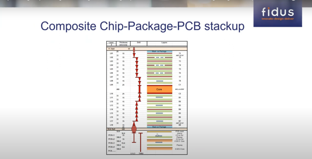
Chip packaging plays a critical role in the signal path. Optimizing chip packaging ensures efficient data transmission with minimal signal degradation. Three key parameters significantly impact signal integrity in high-speed systems:
The PCB, or Printed Circuit Board, acts as the physical platform that connects various electronic components. Signal integrity refers to the ability of the PCB to transmit signals with minimal distortion. In high-speed applications, maintaining excellent signal integrity becomes paramount. Here are some best practices for PCB design in this context:
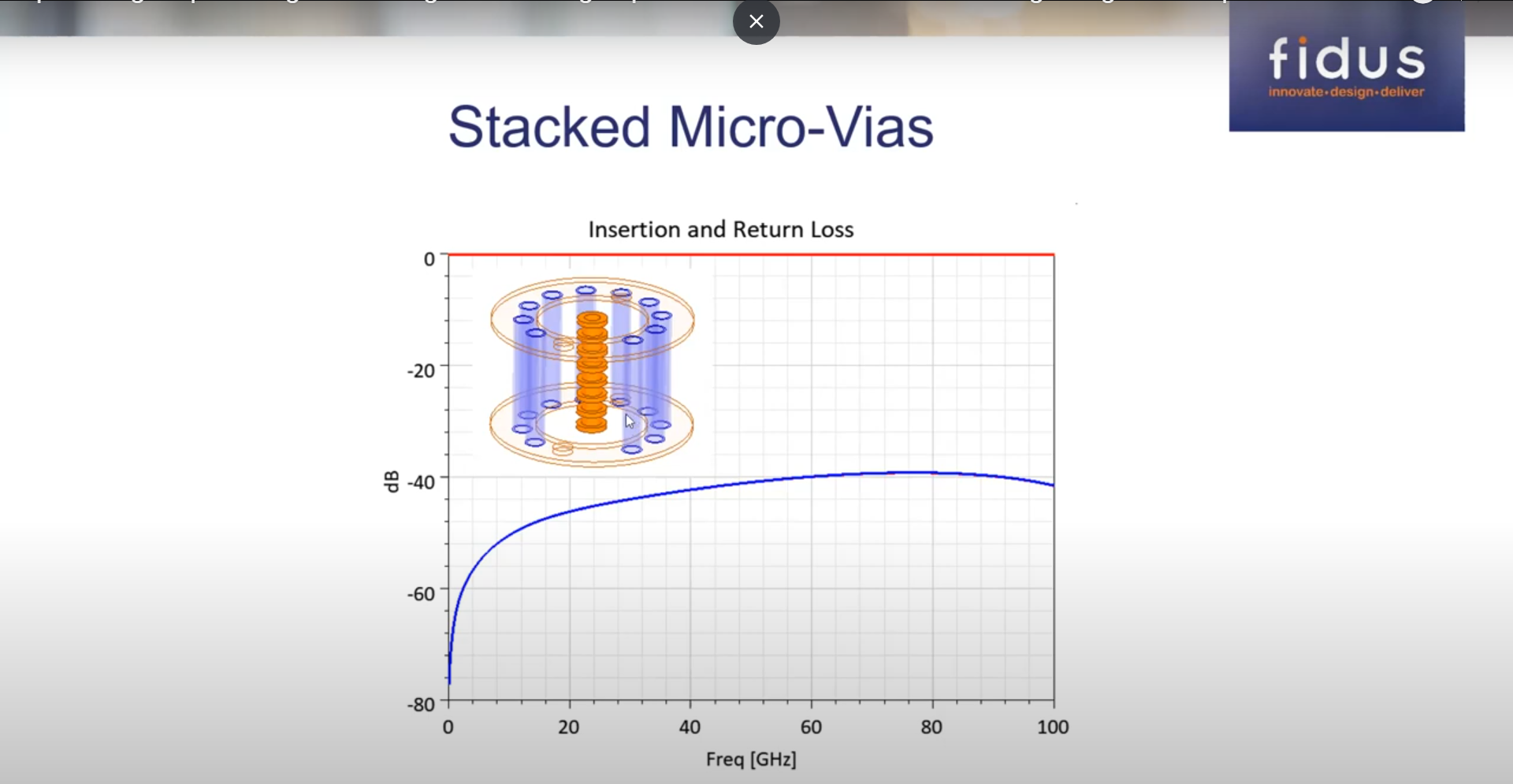
S-parameter simulation is a valuable tool for chip packaging and PCB design. S-parameters represent the electrical behavior of a network at specific ports. By simulating the chip-package interconnect using S-parameters, engineers can predict its performance and identify potential issues before physical fabrication. However, the webinar presented by Syed Bokhari highlights the limitations of S-parameters at high frequencies due to complex electromagnetic interactions within the structure.
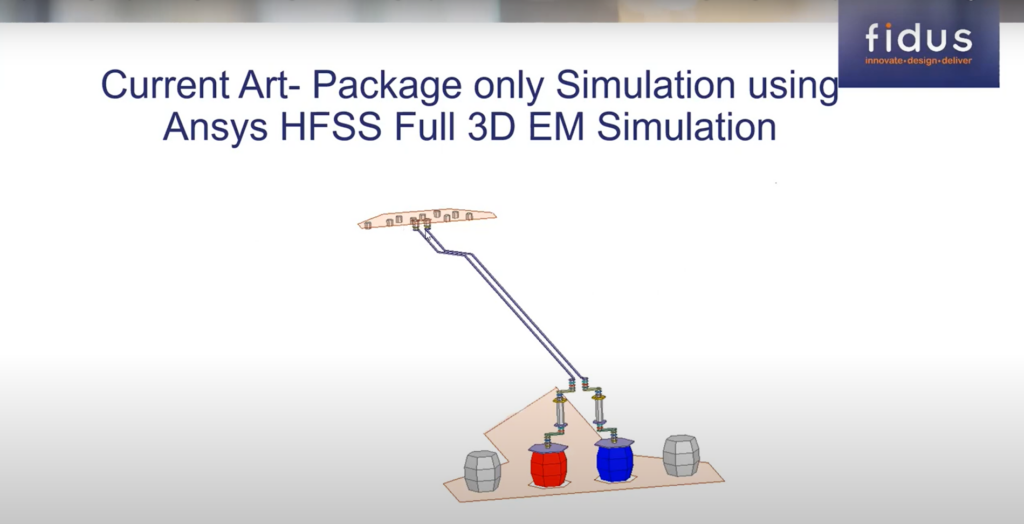
Traditional S-parameter simulation practices often involve simulating the package in isolation, neglecting the critical chip-package-PCB interface. This approach can lead to inaccurate results at high frequencies. To overcome these limitations, the webinar proposes a two-step optimization approach:
In need of similar technical expertise for your high- speed data transmission project?
Contact us today.
The rapid advancement in technology and the push towards higher frequencies are setting new benchmarks in electronic system design. Through a comprehensive understanding of chip packaging, PCB design, and advanced simulation techniques, engineers are better equipped to tackle the challenges posed by high-speed data transmission. The insights and methodologies discussed in this blog, derived from Syed Bokhari’s webinar, provide a robust framework for optimizing electronic systems to meet the demands of tomorrow.
In conclusion, as we navigate the evolving landscape of high-speed data technology, Fidus Systems stands at the forefront, offering innovative solutions that address complex challenges in chip packaging and PCB design. With their advanced S-parameter simulation capabilities and proven track record in transformative projects, Fidus is uniquely positioned to enhance the performance and reliability of your high-speed systems. .
By partnering with Fidus Systems, you gain access to cutting-edge technology and expert guidance, ensuring your projects not only meet but exceed the rigorous demands of modern data transmission requirements. Explore how Fidus Systems can propel your next project to the forefront of the industry.
Reach out to Fidus Systems today to access specialized expertise in high-speed data transmission and take your projects to the next level.

High-bandwidth, low-latency solutions come with tradeoffs. To find the right solution for 3D visualization, consider the following requirements:
Today’s analysis and emulation of genetic sequences demands a low-latency, high-bandwidth solution to transfer massive amounts of data between processors.
Creating a differentiated product takes a thoughtful approach to heterogeneous computing.
Trust us to deliver on time. That’s why 95% of our customers come back.