Addressing Challenges in Chip-Package Interconnect Design for High-Speed Data Transmission
In the fast-paced world of electronic design, understanding and optimizing the intricate dance of high-speed data transmission and PCB signal integrity is crucial. This blog post explores the complexities encountered when designing chip-package interconnects for high-frequency systems operating at and above 50 GHz by Syed Bokhari.
Understanding the Challenges: High-Speed Data and Traditional Methods
At lower frequencies, engineers can rely on established assumptions and design practices for chip packaging and PCBs. However, as we approach the 60 GHz threshold, these assumptions break down. Seemingly straightforward concepts like cable impedance become more nuanced, requiring a deeper understanding of the physical realities within the system. This is where chip packaging optimization and advanced design techniques come into play.
Optimizing Chip Packaging for High-Frequency Performance
Chip packaging plays a critical role in the signal path. Optimizing chip packaging ensures efficient data transmission with minimal signal degradation. Three key parameters significantly impact signal integrity in high-speed systems:
Insertion Loss: This parameter quantifies the power reduction experienced by a signal as it travels through the interconnect. While primarily influenced by physical constraints like trace width and substrate material properties, insertion loss offers limited opportunities for optimization.
Return Loss: In contrast, return loss plays a crucial role in ensuring error-free transmission. It measures the amount of signal power reflected back towards the source due to impedance mismatches. Optimizing return loss minimizes these reflections, creating a more predictable signal path and reducing transmission errors.
Crosstalk: This parameter refers to the unwanted electrical coupling between adjacent signal traces. Crosstalk can distort the intended signal and contribute to transmission errors. Mitigation strategies for crosstalk include increasing trace separation or employing differential signaling techniques.
PCB Design and Signal Integrity: Maintaining a Clean Signal Path
The PCB, or Printed Circuit Board, acts as the physical platform that connects various electronic components. Signal integrity refers to the ability of the PCB to transmit signals with minimal distortion. In high-speed applications, maintaining excellent signal integrity becomes paramount. Here are some best practices for PCB design in this context:
Controlled Impedance Lines: Utilizing controlled impedance lines ensures consistent signal propagation characteristics throughout the PCB.
Minimizing Via Count: Vias, which are connection points through the PCB layers, can introduce signal discontinuities. Minimizing via count helps maintain signal integrity.
Proper Grounding: A well-defined and continuous grounding plane provides a reference point for the signals, minimizing noise and crosstalk.
S-Parameter Simulation: Modeling and Analyzing Interconnect Behavior
S-parameter simulation is a valuable tool for chip packaging and PCB design. S-parameters represent the electrical behavior of a network at specific ports. By simulating the chip-package interconnect using S-parameters, engineers can predict its performance and identify potential issues before physical fabrication. However, the webinar presented by Syed Bokhari highlights the limitations of S-parameters at high frequencies due to complex electromagnetic interactions within the structure.
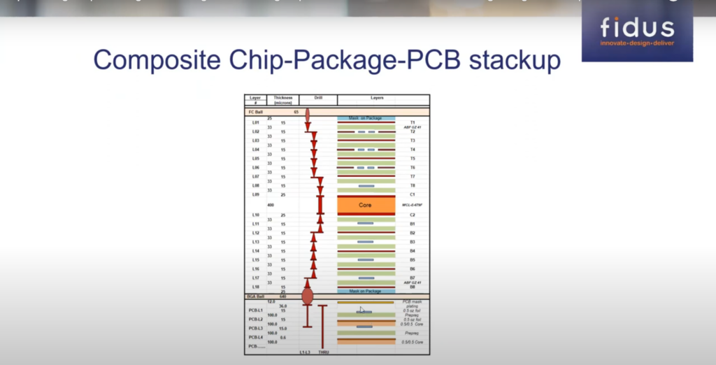
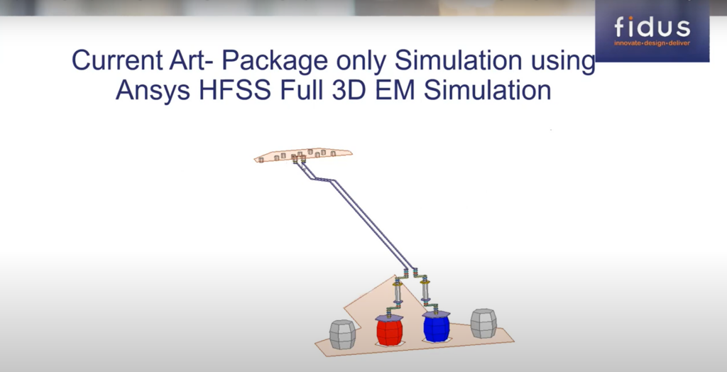
Traditional S-parameter simulation practices often involve simulating the package in isolation, neglecting the critical chip-package-PCB interface. This approach can lead to inaccurate results at high frequencies. To overcome these limitations, the webinar proposes a two-step optimization approach:
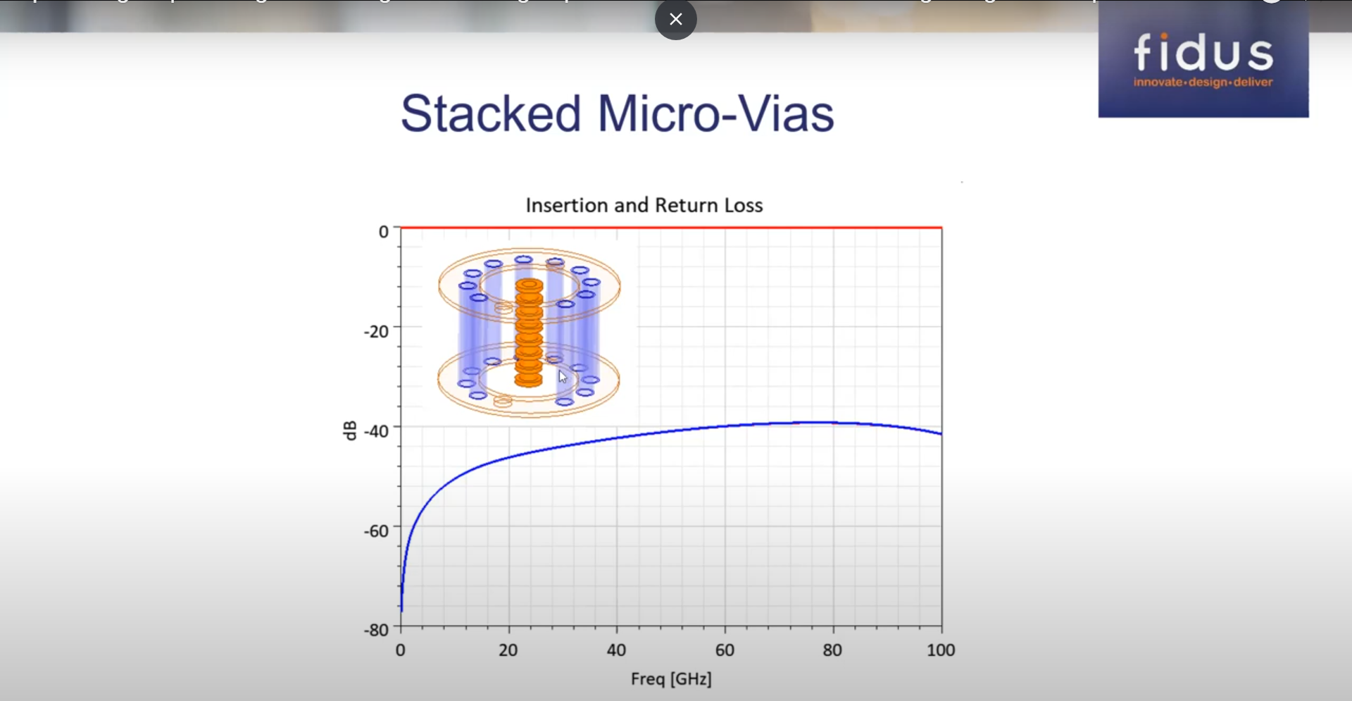
Piecewise Optimization: Break down the complex chip-package-PCB structure into smaller, more manageable sections, such as stacked vias, microvias, and transmission lines. Each section can then be individually optimized to achieve its desired electrical characteristics.
Integrating Optimizations: Once the individual sections are optimized, integrate these optimizations into the complete chip-package-PCB structure using advanced simulation tools like ANSYS HFSS, which can handle full 3D electromagnetic simulations.
In need of similar technical expertise for your high- speed data transmission project? Contact us today.
Conclusion: The Future of High-Speed Data Transmission
The rapid advancement in technology and the push towards higher frequencies are setting new benchmarks in electronic system design. Through a comprehensive understanding of chip packaging, PCB design, and advanced simulation techniques, engineers are better equipped to tackle the challenges posed by high-speed data transmission. The insights and methodologies discussed in this blog, derived from Syed Bokhari’s webinar, provide a robust framework for optimizing electronic systems to meet the demands of tomorrow.
In conclusion, as we navigate the evolving landscape of high-speed data technology, Fidus Systems stands at the forefront, offering innovative solutions that address complex challenges in chip packaging and PCB design. With their advanced S-parameter simulation capabilities and proven track record in transformative projects, Fidus is uniquely positioned to enhance the performance and reliability of your high-speed systems. .
By partnering with Fidus Systems, you gain access to cutting-edge technology and expert guidance, ensuring your projects not only meet but exceed the rigorous demands of modern data transmission requirements. Explore how Fidus Systems can propel your next project to the forefront of the industry.
Reach out to Fidus Systems today to access specialized expertise in high-speed data transmission and take your projects to the next level.
From Classroom to Career: Inside the Fidus × Carleton University FPGA Learning Initiative
Fidus is partnering with Carleton University to support hands-on FPGA education through industry-aligned hardware, practical learning environments, and direct exposure to modern design workflows. This collaboration reflects a shared commitment to strengthening Canada’s engineering talent pipeline and bridging the gap between academic learning and real-world embedded-system development.
The Engineering Capacity Playbook: When, Why, and How to Scale With Embedded Design Expertise
Engineering leaders are under increasing pressure to deliver more complex systems with fewer internal resources. FPGA logic grows more demanding, embedded software expands faster than teams can staff, and board level designs now require deeper integration across hardware and firmware. This playbook gives leaders a clear framework for understanding when external engineering support becomes essential, how to choose an engagement model that protects quality and schedule, and what separates productive collaborations from the ones that create risk. Drawing on lessons from hundreds of advanced development programs, it outlines how to scale engineering capacity without slowing execution or sacrificing control.
What to Expect When Partnering with an Embedded Systems Design Services Company
Hardware doesn’t move at software speed — and that’s okay. Here’s what decision-makers need to know about realistic timelines when partnering with an embedded systems design services company like Fidus.