In the rapidly advancing domain of FPGA design, optimizing performance and efficiency is crucial for companies seeking to innovate and remain competitive. This blog delves into the essential strategies for optimizing FPGA designs using AMD Versal Adaptive SoCs, focusing on high-speed data transfer, dynamic function exchange (DFX), and quality of service (QoS) implementation. With insights from Fidus Systems’ recent webinar led by Normand Leclerc, a seasoned FPGA Designer, we explore the intricacies of enhancing your FPGA designs to achieve superior performance and efficiency.
Here, engineers and decision-makers will learn not only how to leverage AMD Versal Adaptive SoCs for custom FPGA solutions but also how to implement advanced techniques that bring their high-complexity FPGA designs to life.
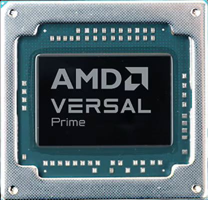
Understanding AMD Versal Adaptive SoCs
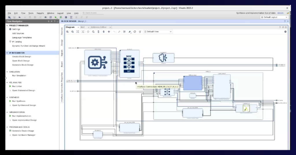
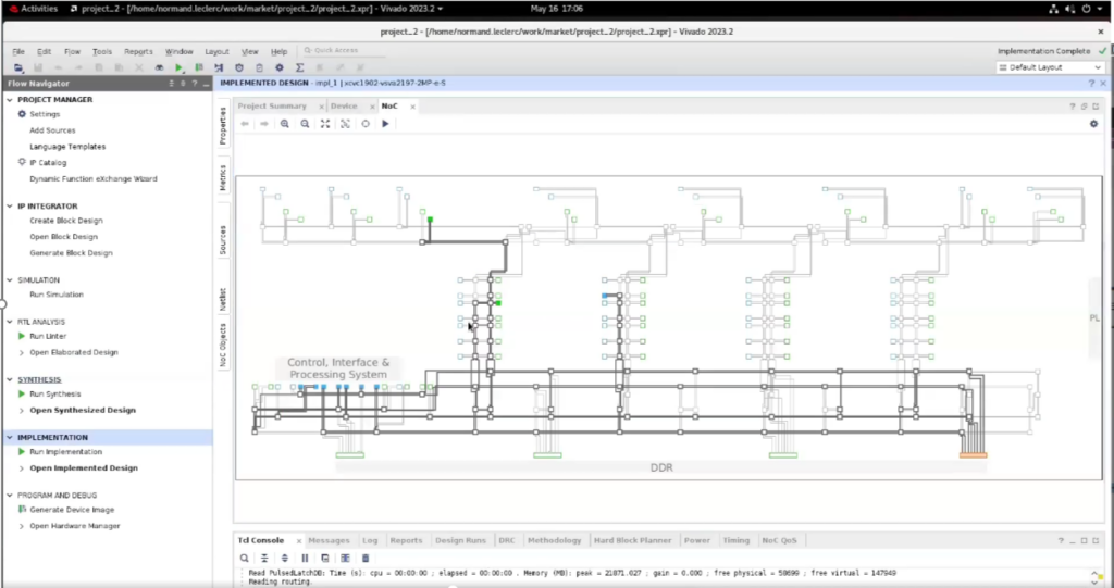
AMD Versal Adaptive SoCs integrate high-speed interfaces such as PCIe, multi-Gigabit Ethernet, and memory controllers, along with numerous I/Os. These components are distributed around the die, with the adaptable engine, programmable logic (PL), at the center. This layout can present challenges, particularly when moving data across the SoC.
To address these challenges, AMD Versal Adaptive SoCs include a high-speed network on chip (NoC). The NoC can transfer data at up to one gigahertz on a 128-bit data bus and features integrated high-efficiency DDR4 and LPDDR4 memory controllers. Some models also include HBM memory controllers. The NoC supports bandwidth allocation and multiple levels of quality of service (QoS), ensuring efficient data transfer across the SoC.
High-Speed Data Moving Application Example
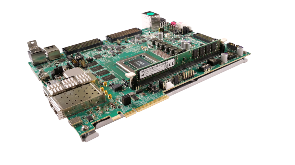
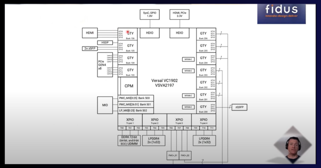
One practical example of optimizing data transfer in Versal SoCs is a high-speed data moving application. This involves capturing 8K video resolution at 60 frames per second, which translates to 48 gigabits per second of video data. The AMD VCK190 evaluation kit is ideal for this application, featuring multiple interfaces such as PCIe Ethernet, HDMI ports, and LPDDR memory.
Project Configuration
In this example, data is transferred from HDMI transceivers to LPDDR memory using the NoC. The project configuration involves selecting appropriate AXI interfaces, configuring memory controller ports, and setting up QoS to ensure efficient data flow. This approach demonstrates the NoC’s ability to handle high-speed data movement effectively.
Detailed NoC Configuration
Configuring the NoC involves several key steps:
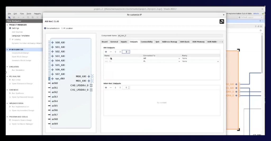
Input and Output Configuration:
Associating AXI Interfaces: Assign each slave AXI interface to its corresponding peripheral. For example, the first interface may be cache-coherent, while others handle non-coherent and low-power domain interfaces.
Connecting Masters: Connect the master AXI interfaces to key components like AI engines and the HDMI frame grabber.
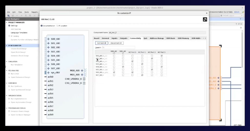
Connectivity Matrix:
Defining Paths: Specify which slave AXI interfaces can access which master interfaces. This ensures data can be routed efficiently to its destination.
Quality of Service (QoS) Settings: Configure QoS to prioritize critical data transfers. For instance, video data may require isochronous QoS to guarantee timely delivery.
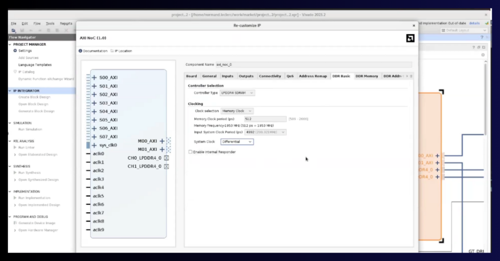
Memory Controller Configuration:
Setting Base Addresses: Define base addresses for memory controllers to manage data storage.
Configuring Timings: Set timings for DDR chips and enable ECC memory if necessary.
Step-by-Step Guide for Configuration:
Input Configuration:
Open the NoC configuration tool and select the board (e.g., VCK190).
Assign each AXI interface to the correct peripheral (e.g., cache-coherent, non-coherent, LPD, and video feed).
Output Configuration:
Define the master AXI interfaces, ensuring connections to AI engines and the HDMI frame grabber are correctly set.
Connectivity and QoS:
Use the connectivity matrix to assign data paths, ensuring high-priority data like video feeds have guaranteed bandwidth.
Configure QoS settings, such as isochronous for video data, to maintain consistent performance.
Memory Controller:
Set base addresses and configure memory timings to ensure optimal data access and storage.
Implementing Quality of Service (QoS)
Implementing QoS is critical for applications with specific latency and bandwidth requirements. In the high-speed data moving example, isochronous QoS is used for video data to guarantee maximum latency, ensuring timely delivery of video frames. Other types of QoS, such as high priority or best effort, can be configured based on the application’s needs.
Steps to Implement QoS:
Identify Traffic Types: Categorize traffic based on latency and bandwidth requirements.
Assign QoS Levels: Apply appropriate QoS levels (e.g., isochronous, high priority) to different traffic types.
Monitor and Adjust: Continuously monitor QoS performance and make adjustments to optimize data flow.
Detailed QoS Implementation:
Categorize Traffic:
Identify critical data flows, such as video feeds, that require low latency and high bandwidth.
Categorize control signals and less critical data separately.
Configure QoS:
Use the NoC configuration tool to assign QoS levels to each data flow.
Set isochronous QoS for video feeds to guarantee timely data transfer.
Monitor Performance:
Use monitoring tools to track QoS performance.
Adjust settings as needed to ensure optimal data flow and system efficiency.
Conclusion
Optimizing FPGA designs with AMD Versal Adaptive SoCs involves leveraging the NoC for efficient data transfer, configuring system components effectively, and implementing QoS to meet specific application requirements. By following these strategies, engineers can achieve high performance and efficiency in their FPGA projects.
Expand your knowledge with these additional resources from our website:
Build for Zynq UltraScale+: Learn how Fidus can help you leverage the advanced capabilities of Zynq UltraScale+ for your projects, ensuring optimized performance and reduced development time.
Build for AMD Versal Adaptive SoCs & FPGAs: Discover our specialized services for AMD Versal Adaptive SoCs and FPGAs, designed to enhance your design efficiency and overall project success.
AMD Partner Page: Explore the benefits of our strong partnership with AMD, providing you with cutting-edge solutions and support for your FPGA and SoC designs.
Ready to dive deeper into optimizing your FPGA designs with AMD Versal Adaptive SoCs? Gain practical insights and expert strategies by exploring our detailed resources and demonstrations. Watch Now to unlock the full potential of your FPGA designs.
For further assistance or questions, our team of FPGA design experts is here to help. Contact us today to discuss your specific challenges and how we can support your FPGA design projects.
How Embedded Systems Outsourcing Differs from Software Outsourcing?
Software outsourcing has a mature playbook. It starts breaking the moment hardware enters the picture. Here is where embedded engagements diverge on toolchains, testing, and the cost of an error, and how to adjust your vendor management before a firmware bug turns into a board respin.
How Do You Deploy a Person Re-Identification Application on AMD Ryzen™ AI?
Discover how Fidus’ Person Re-Identification demo on a Ryzen™ AI–based SAPPHIRE EDGE AI Mini-PC highlights AI integration, optimization, custom-data training, and repeatable testing for faster product development.