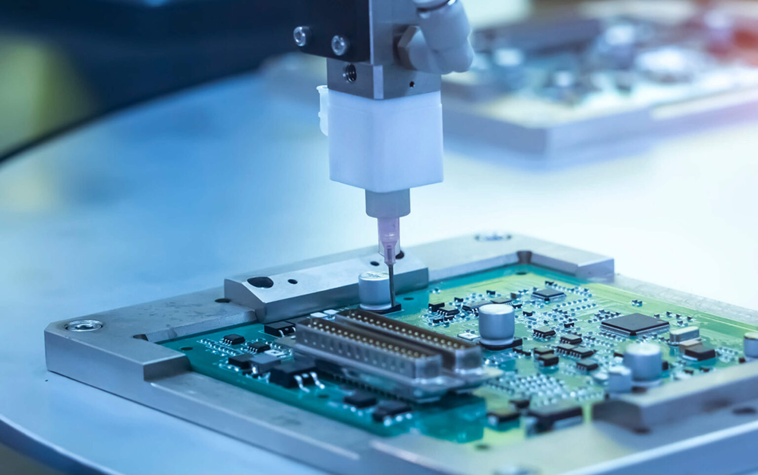
As embedded systems and FPGA designs continue to grow in complexity, engineers are constantly seeking ways to maximize the capabilities of the hardware they work with. Understanding the intricacies of AMD Zynq UltraScale+MPSoC and RFSoC platforms—especially the use of Multiplexed Input/Output (MIO)—is essential for optimizing performance, reducing time-to-market, and ensuring seamless hardware-software integration.
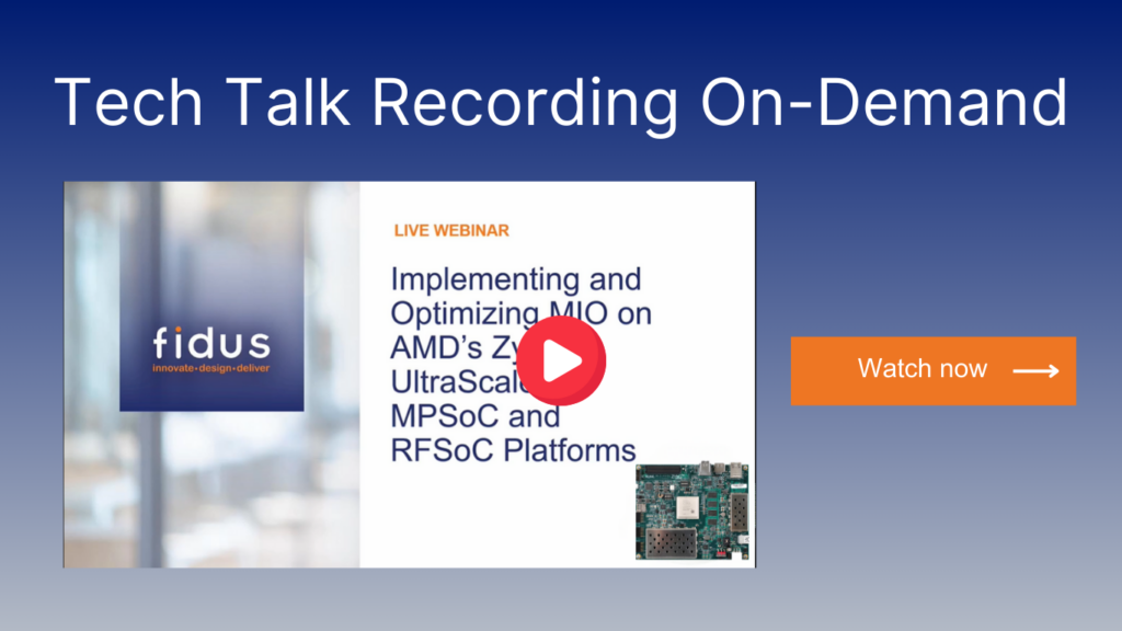
In our latest TechTalk, Implementing and Optimizing MIO on AMD Zynq UltraScale+ MPSoC and RFSoC Platforms, Scott Turnbull, CTO of Fidus Systems, and Jeremy Brooks, Senior Embedded Software Engineer, shared invaluable insights on how to effectively configure and utilize MIO for your projects. With decades of design expertise and over 50 successful Zynq UltraScale+ projects under our belt, Fidus is uniquely positioned to help you tackle the most challenging aspects of embedded system design.
Understanding MIO: The Backbone of Peripheral Integration
What is MIO? A Foundation for Embedded Innovation
MIO, or Multiplexed Input/Output, is a set of configurable pins on Zynq UltraScale+ devices. These pins are dedicated to connecting external peripherals to the Processing System (PS), which houses fixed-function blocks like Ethernet MACs, USB controllers, SPI interfaces, and more.
Unlike the FPGA programmable logic (PL) portion of the chip, MIO is tied to the PS and supports specific hard peripherals. This makes MIO an efficient, power-saving option for interfacing with external hardware while leaving the PL available for high-performance, customizable functions.
78 Configurable Pins: Divided across three banks with user-definable voltages.
Broad Peripheral Support: Enables SPI, QSPI, I²C, UART, Gigabit Ethernet, USB, and more.
High-Speed Capabilities: Works alongside up to four PS Gigabit Transceivers (GTRs) for PCIe, USB 3.0, and DisplayPort.
Efficient Resource Use: Leverages PS resources to reduce PL utilization and power consumption.
The Importance of Optimization:
Optimizing MIO configuration is crucial for several reasons:
Enhanced Performance: Proper mapping ensures low-latency communication between the PS and external devices.
Reduced Power Consumption: PS peripherals consume significantly less power compared to implementing equivalent functions in the FPGA fabric.
Design Scalability: By freeing up PL resources, you can scale your designs for future requirements.
However, MIO assignments come with limitations—certain peripherals can only map to specific pins. Understanding these constraints and planning accordingly is key to avoiding design bottlenecks. Fidus, an expert in FPGA design, embedded software, and more. delivers precision-driven solutions through their “First-Time-Right” approach, ensuring that designs are optimized from the start.
MIO pins are organized into three banks—each powered by a separate voltage rail (VCC_PS_IO). All pins within a bank must share the same voltage level, making voltage planning a key step in advanced designs.
Bank 500 (MIO 0–25): Configurable for 1.8V or 3.3V.
Bank 501 (MIO 26–51): Voltage must remain uniform across all pins.
Bank 502 (MIO 52–77): Independent voltage configuration.
Advanced Application
In multi-peripheral systems, group high-speed interfaces (e.g., Ethernet or USB) into one bank with 3.3V, while reserving 1.8V banks for low-power communication protocols like I²C or UART.
Use external voltage level shifters sparingly to avoid additional power consumption and latency.
Pro Tip: Consider future expandability. Designing with consistent voltage standards across banks simplifies later hardware modifications.
Step 2: Maximizing Pin Efficiency Through PS and PL Collaboration
While MIO provides the first line of access to peripherals, advanced systems often combine MIO and Extended MIO (EMIO) to unlock additional connectivity. EMIO enables the use of programmable logic (PL) pins to extend peripheral access when MIO pin counts are exhausted.
Advanced Application
In high-I/O systems, such as multi-Ethernet port gateways, leverage EMIO to route overflow peripheral traffic through the PL. Use Vivado’s pin planner to ensure that EMIO latency and signal integrity remain within acceptable limits.
Utilize PL-based GPIO for custom peripherals, reserving MIO for standardized PS hard peripherals to minimize complexity.
Challenge: Understand the limitations of EMIO, including potential clock synchronization issues when crossing the PS-PL boundary.
Step 3: Optimizing High-Speed GTR Assignments
For applications requiring high-speed data transfer—such as PCIe, USB 3.0, or DisplayPort—Gigabit Transceivers (GTRs) offer unparalleled performance. However, GTRs have strict lane mapping rules that must align with peripheral requirements.
Advanced Application
Map PCIe lanes for x4 configurations to GTRs in strict ordinal order (e.g., Lane 0 to GTR 0, Lane 1 to GTR 1). Mismatches in mapping can cause data integrity issues.
For USB 3.0 SuperSpeed, assign TX/RX pairs to GTRs closest to their MIO-based control signals to minimize trace lengths and signal degradation.
Pro Tip: Use Vivado’s signal integrity tools to model GTR performance and verify compliance with high-speed protocol specifications.
Step 4: Leveraging the MIO Table for Complex Configurations
The MIO mapping table in AMD’s Technical Reference Manual (TRM) is an essential tool for advanced MIO optimization. This table outlines the specific pin ranges for every PS peripheral and their corresponding MIO assignments.
For instance:
Ethernet GEM 1: Assignable to MIO 38–49.
Dual QSPI: Requires MIO 0–12 for implementation.
USB 3.0 SuperSpeed: Maps control signals to MIOs while routing TX/RX pairs to Gigabit Transceivers (GTRs).
Advanced Application
For high-density designs, prioritize frequently accessed peripherals (e.g., QSPI for boot storage) on contiguous MIO pin ranges. This simplifies routing and reduces trace crosstalk.
Use underutilized peripherals (e.g., secondary UARTs) to fill gaps in MIO pin allocation, ensuring no pins go to waste.
Pro Tip: When assigning MIO, ensure each pin aligns with its function (e.g., chip select, data, or clock) as outlined in the QSPI controller section of the TRM.
Step 5: Validate Assignments with Tools
Using AMD’s tools is critical for ensuring your MIO configuration meets design requirements:
Vivado IDE: Use the I/O Configuration Tool to assign pins and resolve conflicts.
Vitis IDE: Verify hardware mappings and check compatibility with software drivers.
PetaLinux Tools: Automatically generate device trees for Linux-based designs, simplifying integration with default drivers.
Watch the full webinar for an in-depth exploration of these MIO optimization steps, complete with expert insights and practical applications.
Common Challenges in MIO Design and Solutions
Challenge
Description
Solution
Peripheral Conflicts
Limited to 78 MIO pins, multiple peripherals may compete for the same resources (e.g., NAND Flash vs. QSPI).
– Use Vivado’s I/O Configuration Tool to identify and resolve conflicts. – Prioritize critical peripherals.
Voltage Mismatches
Devices with different voltage requirements cannot share the same MIO bank.
– Group peripherals with similar voltage needs into the same bank. – Use external level shifters for mixed-voltage systems.
Complex High-Speed Configurations
Improper GTR assignments for protocols like PCIe and DisplayPort can lead to performance issues.
– Refer to AMD’s GTR mapping tables for guidance. – Validate configurations using Vitis IDE to ensure proper alignment of clock sources and data lanes.
This table highlights the most common challenges engineers face and actionable solutions to ensure seamless MIO integration.
Practical Applications
Industrial IoT Gateways: IoT gateways require a mix of Ethernet, UART, and I²C connections to communicate with edge devices and centralized control systems. By grouping Ethernet in one voltage bank and offloading UART to EMIO, engineers can design scalable gateways that handle high data throughput with minimal latency.
Video Processing Systems: Video applications demand fast memory access and robust data transmission. MIO supports QSPI for memory and Ethernet for streaming, while GTRs enable USB 3.0 SuperSpeed for external cameras and storage.
Edge AI Accelerators: Edge AI solutions rely on PCIe for connecting AI accelerators, Ethernet for cloud communication, and GPIO for hardware control. Strategic MIO and GTR assignments ensure real-time data processing and efficient power management.
Aerospace and Defense Systems: In mission-critical environments, MIO enables secure boot via QSPI, diagnostics through USB, and reliable communication with sensors. Voltage planning and conflict-free peripheral mapping are essential for meeting stringent reliability requirements.
Medical Imaging Devices: Medical systems such as MRI and ultrasound machines utilize Ethernet for transmitting imaging data, QSPI for software storage, and UART for maintenance. Optimizing MIO assignments ensures these devices operate seamlessly under demanding workloads.
Automotive Infotainment: Modern vehicles rely on DisplayPort for high-resolution displays, USB for data transfer, and Ethernet for connectivity. By optimizing MIO and GTR assignments, infotainment systems can deliver smooth user experiences without compromising reliability.
Prioritizing PS MIO vs. PL GPIO: Use PS MIO first for critical peripherals to simplify design and maximize efficiency. Resort to PL GPIO only for tasks requiring higher flexibility or speed.
TRM Navigation Tips: Focus on specific sections relevant to your project, such as Ethernet or USB controllers. Key tables in the TRM can save time and prevent design errors.
Planning for Scalability: Assign peripherals like I²C and Ethernet with future expansion in mind. Reserve one controller or use EMIO to maintain flexibility for future additions.
Real-World Optimization: MIO mapping improvements enabled faster data transfer in IoT gateways, seamless video processing, and efficient Edge AI designs.
Overcoming Integration Challenges: Early collaboration between FPGA and software teams ensures smoother integration and avoids costly redesigns.
The MIO subsystem on AMD Zynq UltraScale+ platforms is a powerful enabler for embedded systems, offering a structured yet flexible way to connect peripherals while preserving resources for advanced tasks. By understanding its capabilities and leveraging optimization strategies, engineers can design systems that are not only efficient but also scalable and future-ready.
Whether you are developing IoT gateways, video systems, or edge AI solutions, MIO is a crucial part of the architecture. To learn more about unlocking its full potential, watch our TechTalk and explore the tools and techniques used by industry leaders.
How Embedded Systems Outsourcing Differs from Software Outsourcing?
Software outsourcing has a mature playbook. It starts breaking the moment hardware enters the picture. Here is where embedded engagements diverge on toolchains, testing, and the cost of an error, and how to adjust your vendor management before a firmware bug turns into a board respin.
How Do You Deploy a Person Re-Identification Application on AMD Ryzen™ AI?
Discover how Fidus’ Person Re-Identification demo on a Ryzen™ AI–based SAPPHIRE EDGE AI Mini-PC highlights AI integration, optimization, custom-data training, and repeatable testing for faster product development.