The path from early driver aids to advanced driver assistance systems (ADAS) has been a steady climb toward greater vehicle autonomy. The earliest systems, such as anti-lock braking (ABS) and early traction control, were reactive technologies. They functioned in isolation, relying on electromechanical feedback loops to respond to specific events, such as wheel slip or changes in brake pressure. Processing was minimal, with no real capacity to interpret a broader driving context.
Today’s ADAS platforms are far more sophisticated, capable of monitoring the vehicle’s surroundings in real time, interpreting complex traffic scenarios, and even anticipating potential hazards. This leap is powered by embedded systems that integrate multiple sensing modalities—radar for range and velocity, cameras for object classification, LiDAR for high-precision mapping, and ultrasonic sensors for short-range awareness. The embedded processors at the core of these systems must process and analyze gigabits of data per second, transforming raw signals into actionable intelligence in milliseconds.
The evolution of intelligence in modern vehicles
If radar is part of your ADAS strategy, our white paper Best Practices for Developing Cost-Effective FPGA-Based DSP Architecture for 8-Channel FMCW Radar in ADAS offers practical design guidance.
It covers high-bandwidth DDR DRAM interfaces, essential DSP algorithms, and strategies to balance performance with cost in multi-channel radar systems.
At Fidus, we design the embedded frameworks that make this possible. By combining expertise in FPGA, ASIC, MPSoC, and embedded software, we create architectures that handle high data throughput, low-latency decision-making, and safety compliance in a single, robust platform. This ensures that ADAS features, whether adaptive cruise control, lane-keeping assist, or automated emergency braking, respond with precision and reliability in real-world conditions.
The architecture behind ADAS innovation
The foundation of modern ADAS lies in architectures that can collect, process, and act on sensor data without delay. A core technology in this stack is Frequency-Modulated Continuous-Wave (FMCW) radar, valued for its ability to measure distance, velocity, and angle in all weather and lighting conditions. On its own, radar is powerful, but in advanced systems, it works alongside LiDAR for precise 3D mapping and cameras for object recognition, with data fused to create a complete, reliable model of the vehicle’s surroundings.
This fusion can be handled by distributed ECUs, where each sensor processes its own data locally, or by centralized controllers that aggregate and process inputs from multiple sensors. Centralized approaches offer better coordination and decision-making but demand high-bandwidth memory systems and low-latency interconnects to prevent processing bottlenecks.
Fidus engineers design both distributed and centralized architectures, optimizing data paths, memory subsystems, and processing workloads so that ADAS functions operate in real time even under the heaviest sensor loads.
Signal processing: the brain behind ADAS operations
For radar-based ADAS, the signal processing chain is where raw sensor data becomes actionable intelligence. In an FMCW radar system, the embedded processor interprets reflected signals to determine an object’s range, velocity, and angle. These operations must happen in real time, often across multiple channels, while filtering noise and managing interference from other vehicles and environmental sources.
The challenge is processing these large, continuous data streams without introducing latency. This is where FPGA-based architectures excel, offering massive parallelism for range-Doppler processing and angle-of-arrival calculations. Advanced algorithms—such as CFAR detection for consistent target sensitivity and Kalman filtering for stable tracking—are implemented directly in hardware to keep performance predictable.
Fidus specializes in mapping these workloads efficiently to FPGA resources, ensuring that signal processing remains fast, accurate, and reliable even in complex, high-traffic environments.
Hardware and software synergy in ADAS
ADAS platforms rely on tight coordination between high-performance hardware and the software frameworks that control it. FPGAs are often used for computationally intensive operations such as radar signal processing and sensor fusion because they can handle multiple data streams in parallel with minimal latency. Paired with high-bandwidth DDR or LPDDR memory interfaces, they keep sensor data moving without interruption.
On the software side, real-time operating systems (RTOS) and automotive middleware ensure deterministic execution, allowing safety-critical functions to run reliably under varying conditions. Effective integration requires careful alignment between hardware capabilities and software algorithms, as mismatches can introduce delays or degrade accuracy. This hardware-software co-design approach is essential for meeting both performance targets and functional safety requirements in modern ADAS.
Future-proofing ADAS development
As vehicle autonomy advances, ADAS platforms must be designed to adapt to higher sensor resolutions, more complex algorithms, and stricter safety regulations. Scalable architectures allow hardware to accommodate future processing demands without requiring a complete redesign, while modular software frameworks make it easier to update features and incorporate new sensing technologies.
Cybersecurity is becoming as critical as functional safety, with systems required to protect against intrusion, ensure secure boot processes, and comply with standards such as UNECE WP.29 and ISO 21434. At the same time, fail-operational designs are gaining importance—systems must maintain essential functions even in the event of hardware faults or partial failures.
By prioritizing scalability, security, and redundancy during the initial design phase, engineering teams can reduce long-term costs and ensure ADAS platforms remain viable as the industry moves toward higher levels of automation.
Performance optimization and validation
Optimizing ADAS performance is about more than raw processing speed—it’s about achieving consistent, reliable operation within strict automotive power and thermal limits. Processing throughput, memory bandwidth, and algorithm efficiency all have to be balanced against energy consumption, especially in electric vehicles where every watt counts.
Validation is equally critical. Hardware-in-the-loop (HIL) and software-in-the-loop (SIL) testing allow engineers to simulate complex driving scenarios without risking vehicle hardware. Scenario-based testing, using both synthetic and real-world datasets, helps ensure algorithms perform reliably under edge cases such as heavy rain, glare, or dense traffic. Benchmarking against key performance indicators like reaction time, detection accuracy, and false positive rates provides an objective measure of readiness.
A disciplined optimization and validation process ensures that ADAS features meet safety and performance requirements before entering production, reducing risk and improving time to market.
Implementation best practices
Successful ADAS deployment depends on careful planning from concept through production. Early-stage architecture reviews help align performance targets, safety goals, and cost constraints before development begins. Precision calibration during integration ensures sensor alignment and data accuracy, reducing the likelihood of false detections or missed hazards once the system is on the road.
Design choices should balance cost and performance, optimizing hardware resources without sacrificing reliability or compliance with automotive standards. Thorough documentation—covering system architecture, safety analyses, and calibration procedures—not only supports regulatory approvals but also simplifies long-term maintenance and future upgrades.
By following a structured, standards-aligned implementation process, engineering teams can bring robust, scalable ADAS solutions to market more efficiently while maintaining the safety and reliability demanded in automotive applications.
Accelerate radar-based ADAS development with our white paper
Designing an FMCW radar architecture that is both high-performance and cost-effective is a common challenge in ADAS engineering. Our latest white paper provides a detailed, practical framework for meeting that challenge head-on.
This resource outlines a proven FPGA-based design approach for multi-channel FMCW radar, with a focus on:
Achieving sustained throughput with high-bandwidth DDR DRAM interfaces.
Implementing essential DSP algorithms for accurate object detection and tracking.
Balancing performance, scalability, and production cost for automotive deployment.
It’s designed for engineering teams looking to streamline development, reduce risk, and ensure their ADAS radar systems meet both current and future requirements.
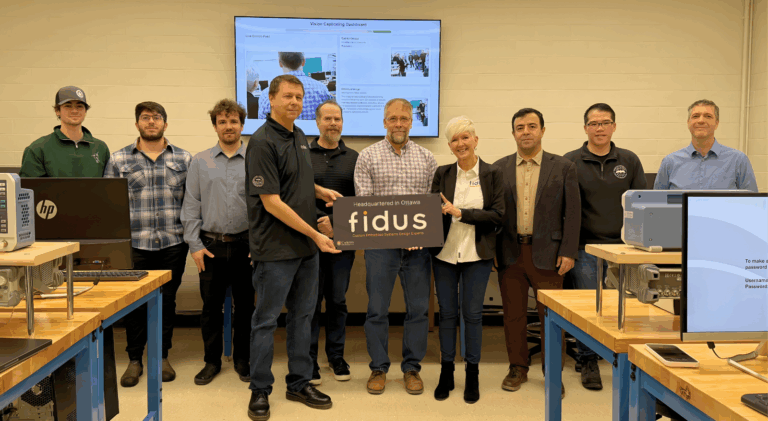
From Classroom to Career: Inside the Fidus × Carleton University FPGA Learning Initiative
Fidus is partnering with Carleton University to support hands-on FPGA education through industry-aligned hardware, practical learning environments, and direct exposure to modern design workflows. This collaboration reflects a shared commitment to strengthening Canada’s engineering talent pipeline and bridging the gap between academic learning and real-world embedded-system development.
The Engineering Capacity Playbook: When, Why, and How to Scale With Embedded Design Expertise
Engineering leaders are under increasing pressure to deliver more complex systems with fewer internal resources. FPGA logic grows more demanding, embedded software expands faster than teams can staff, and board level designs now require deeper integration across hardware and firmware. This playbook gives leaders a clear framework for understanding when external engineering support becomes essential, how to choose an engagement model that protects quality and schedule, and what separates productive collaborations from the ones that create risk. Drawing on lessons from hundreds of advanced development programs, it outlines how to scale engineering capacity without slowing execution or sacrificing control.
What to Expect When Partnering with an Embedded Systems Design Services Company
Hardware doesn’t move at software speed — and that’s okay. Here’s what decision-makers need to know about realistic timelines when partnering with an embedded systems design services company like Fidus.